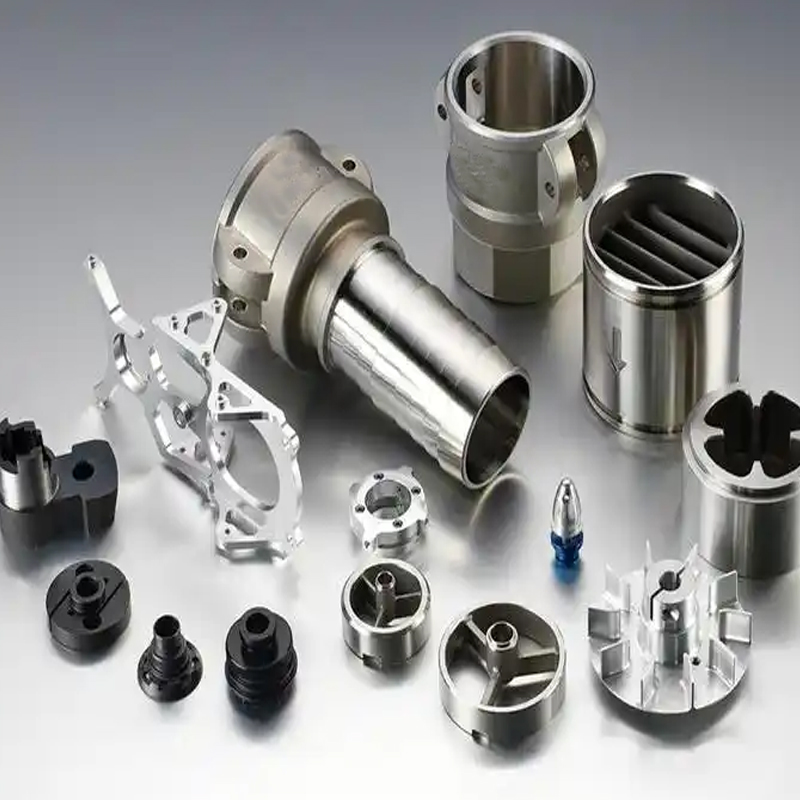
How to achieve precision in semiconductor component processing
The key technology system for achieving nanoscale precision in semiconductor components covers three dimensions: material control, process optimization, and detection verification: 1、 Material preparation and pretreatment Wafer thinning control The original thickness of a 12 inch wafer is 775 μ m, and thinning requires the use of temporary bonding/debonding technology to achieve ultra-thin processing below 20 μ m, with thickness variation controlled within<1 μ m. SiC substrate requirements: Si surface roughness Ra ≤ 0.3nm, C surface Ra ≤ 0.5nm, using a combination of mechanical initial polishing and chemical mechanical precision polishing process. Material stability optimization Perform